Hands-on Electrical Engineering Curriculum at UC San Diego Earns Innovative Program Award
Technology & Engineering
The Electrical and Computer Engineering Department at UC San Diego was recognized for its pioneering hands-on lab curriculum by the leading association for electrical and computer engineering educators in North America.
Barna Saha Celebrated as Harry E. Gruber Endowed Chair at UC San Diego
Milestones
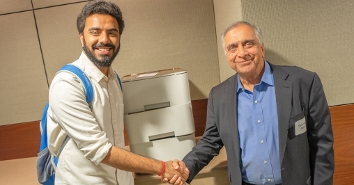
Barna Saha, a computer scientist at UC San Diego who spearheads a new $10 million multi-university research institute to tackle problems in theoretical foundations of data science, was honored this week as the Harry E. Gruber Professor of Computer Science and Information Technologies Endowed Chair.
Leaders in Their Fields
Awards & Accolades
Five UC San Diego graduate students recently joined the ranks of the Bouchet Graduate Honor Society, a prestigious national organization that recognizes scholars whose commitment to social justice, diversity, leadership and academic excellence pushes the boundaries of doctoral education.