

NSF Locates National Nanotechnology Coordinated Infrastructure Site at UC San Diego
Published Date
By:
- Tiffany Fox
Share This:
Article Content
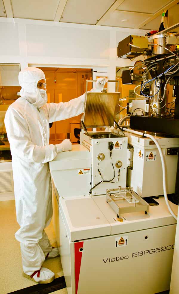
Ryan Anderson, process engineer for the Nano3 facility in the Qualcomm Institute, prepares to remove a sample from the Vistec EBPG5200 electron beam writer.
Ryan Anderson, process engineer for the Nano3 facility in the Qualcomm Institute, prepares to remove a sample from the Vistec EBPG5200 electron beam writer.
San Diego, Calif., Sept. 16, 2015 —The National Science Foundation (NSF), after a lengthy competitive process, has selected the University of California, San Diego to be one the first university sites in the new National Nanotechnology Coordinated Infrastructure (NNCI). The agency will fund UC San Diego $1.1 million annually over five years to advance nanoscale science and engineering and develop transformative nanotechnologies and nanotechnology-based startups.
UC San Diego is the only university in the UC system – as well as the only public university in California – to receive one of 16 NNCI awards (Stanford is the only other California recipient). UC San Diego is also one of few universities to join NNCI that was not previously a member of the National Nanotechnology Infrastructure Network (NNIN), a prior round of NSF funding offered a decade ago for nanoscale science and engineering research. UC San Diego’s Nano3 nanofabrication cleanroom facility – which is based at the University’s Qualcomm Insititute – had not even been built when NNIN began.
“This is a vote of confidence in the advanced infrastructure already deployed by UC San Diego to support nanotechnology research and development, and the NSF support will allow us to play a major role in the new nationwide network,” said UC San Diego Chancellor Pradeep K. Khosla. “Locating the NNCI site on this campus will make it easier for faculty to use existing and new infrastructure, and we will open the door wider to industry users, especially to smaller companies and non-traditional users of nanotechnologies, by offering them capabilities they could not otherwise afford.”
Professor Yuhwa Lo, Director of Nano3, will serve as site director for the new NNCI site at UC San Diego.
To date, more than 110 companies have used the Qualcomm Institute’s 15,000-square-foot Nano3, in addition to users from 180 university groups and national labs.
The UC San Diego NNCI aims to boost corporate use of all of its facilities to reach a 50-50 balance between academic and industry users. The NSF support will also power growth in overall usage of the nano facilities.
“With this support and vote of confidence, we aim to double the annual number of user hours for our combined nanotechnology facilities and maximize the impact of nanotechnologies to as many fields of research and industry sectors as we can reach,” said Yuhwa Lo, principal investigator on the NNCI project at UC San Diego and a professor of Electrical and Computer Engineering (ECE). “To do so, we will invest in multi-purpose, platform technologies that will allow us to offer fabrication-on-demand services to a larger number of users, and to provide extended services for early-stage R&D projects with the low budgets that are typical for startup companies.”
The primary mandate of the NNCI is to “accelerate research towards discovery in nanoscale science, engineering and technology by providing open, affordable access to state-of-the-art nanofabrication tools, characterization instruments and computational resources, and most importantly, by providing expertise in these areas.”
UC San Diego demonstrated to NSF its unique strengths in three nano domains: NanoBioMedicine, NanoPhotonics, and NanoMagnetics. Nano3 and the Chip-Scale Photonics Test Facility are the two multi-user facilities making up the UC San Diego NNCI, and both are located in the Qualcomm Institute. They support research in NanoBioMedicine and NanoPhotonics, with a lot of the work enabled by Nano3’s high-end Vistec electron-beam lithography system, nanoimprinting capabilities, microfluidics technologies, atomic layer deposition process, and a DualBeam cryo-focused ion beam system (one of the few such systems in the U.S. capable of producing cryogenic TEM samples to capture free cellular activity in time).
The Chip-Scale lab recently received a Department of Defense grant to acquire a Raman spectrometry system to characterize nanolasers or test DNA, biomarkers, strained silicon and other nanoscale materials. In NanoMagnetics, UC San Diego boasts several research labs, but none designed to be multi-user facilities, open to industry users. Labs in Physics, ECE, Mechanical and Aerospace Engineering (MAE) and the Center for Memory and Recording Research (CMRR) will collaborate to make their equipment and expertise available through a common NNCI recharge system, in addition to investing in development of state-of-the-art nanomagnetics technologies.
Nano3 Technical Director Bernd Fruhberger, who manages the facility in Calit2’s Qualcomm Institute, says the NSF funding will allow the team to fill up to five staff positions, including one additional Ph.D.-level expert in nanofabrication engineering. “Support staff are critical if the UC San Diego NNCI is going to attract enough corporate users to create the desired 50-50 balance between industry and academia,” said Fruhberger. “One hopeful sign is that 30 percent of our corporate users have fewer than 30 employees each, so we have already proved our worth to those users, and we will now be in an even better position to attract small- and medium-sized businesses that need access to cleanrooms, advanced equipment, and especially the sophisticated staff to make use of them.”
Boosting use of the UC San Diego NNCI facilities is a priority for site leadership. In the near term, faculty and staff intend to focus their effort on recruiting faculty and student users from community colleges (which generally do not have advanced equipment), and from small or startup companies.
In addition to site director Yuhwa Lo and deputy director Shaya Fainman, senior personnel will include NE Prof. Shaochen Chen (who developed his own 3D Bioprinter), Bioengineering Prof. Todd Coleman, and ECE’s Eric Fullerton and Vitaliy Lomakin. Senior staff include Nano3’s Fruhberger (operations) and The von Liebig Entrepreneurism Center director Rosibel Ochoa (business development). Other faculty members hail from the ECE, MAE, Bioengineering, NanoEngineering, Chemistry and Biochemistry and Physics departments, as well as the Division of Biological Science, School of Medicine and the Materials Science and Engineering program.
More than 3,300 people have received training on how to use Nano3 and specific equipment, nearly 20 percent of them as undergraduates, and most of the training is done by Nano3 staff engineers. The UC San Diego NNCI facility will integrate graduate and undergraduate education with research. Extrapolating from current usage of the Nano3 facility, the site anticipates that some 400 M.S. and Ph.D. students will utilize the site annually, and among faculty, increasing numbers of biomedical scientists, including trainees, are expected. The site is budgeting support for 12 Research Experiences for Undergraduates (REU) students each year to work directly with participating site faculty, but organizers intend to apply for additional REU support to provide authentic research experiences for undergraduates within the UC San Diego NNCI site.
The NNCI site will further integrate staff and engineering specialists who support the various nano facilities at UC San Diego in order to make their expertise easier and cheaper to access. They will also develop and share effective methods for efficient management and operation of the site within the national NNCI and from other NNCI sites.
As outlined in the proposal to NSF, the UC San Diego NNCI plans to double annual user hours by making the facilities more attractive in several ways. They plan to expand capabilities in high demand (such as 3D nanoprinting and nanoimprinting on flexible platforms) and by streamlining fabrication-on-demand services for onsite and remote users. They will also clear up bottlenecks by expanding instrumentation and processing capabilities, and encourage access for non-traditional users by developing hands-on training programs that demonstrate the value of NNCI to researchers who are less familiar with nanotechnologies. Finally, the NNCI site will procure or develop new tools and technologies.
The NNCI funding can be directed at those growth areas, in part, because the Qualcomm Institute has agreed to continue covering $400,000 it spends annually on Nano3. “The NNCI site is a feather in the cap of the campus and the institute,” said Qualcomm Institute Director Ramesh Rao. “We will continue to provide support for operating these facilities, and we look forward to establishing new connections among the corporations, national laboratories and other institutions that will now be looking at San Diego as one of the elite locations in the country to do nanotechnology.”
Share This:
You May Also Like


Stay in the Know
Keep up with all the latest from UC San Diego. Subscribe to the newsletter today.