

Accelerating Design Times for High-Performance Systems-on-Chip
Published Date
By:
- Doug Ramsey
Share This:
Article Content
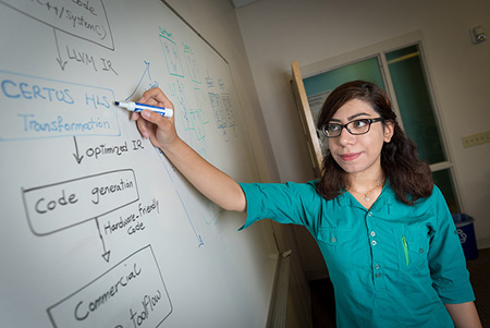
CSE fourth-year Ph.D. student Atieh Lotfi is working on the CERTUS project with advisor Rajesh Gupta, the Principal Investigator on CERTUS.
A team of computer scientists and electrical engineers from four U.S. universities have been awarded a joint project with nearly $5 million in funding from the Defense Advanced Research Projects Agency (DARPA). Led by University of California San Diego computer-engineering professor Rajesh Gupta, the group of nine faculty members -- five from UC San Diego, one each from UCLA and the University of Michigan, and two professors from Cornell University – will develop a “synthesis methodology for accelerator-centric systems-on-chips and tool flows” that goes by the name CERTUS (Latin for definite, trustworthy or reliable).
Productivity involving the time it takes to design systems-on-chips (SoCs) has remained flat, largely because of the design complexity that is also responsible for rapidly rising costs. Indeed, as much as 50 percent of design and verification time must be devoted to designing high-performance analog parts, customized data-paths, and design exploration to meet schedules.
“All parts of chip design from clocking, sensing circuits to integrated data paths and synthesized random logic must come together in complicated tool flows that are, of necessity, hand-crafted to a specific process and process node,” said CERTUS principal investigator Rajesh Gupta. “This causes multiple iterations through various design stages, so we need to come up with new methodologies to achieve a dramatic improvement in design times.”
CERTUS is part of the DARPA Circuit Realization at Faster Timescales (CRAFT) effort, which aims to reduce chip design times to a target 16-week design time for an SoC, including 5 weeks of physical design and closure. That represents a 10x improvement over the current time it takes (~ 160 weeks) to design a custom DoD ASIC chip. However, the researchers aim in their first fab run to demonstrate a 5x reduction, i.e., cutting design time by 80 percent. By the end of the project, they plan to demonstrate a 10x cut in design time, i.e., a 90 percent drop. “Reducing the effort required to design and verify leading-edge CMOS ASICs is critical to development of next-generation defense systems that require high computational performance in a power-constrained environment,” said DARPA Microsystems Technology Office (MTO) Program Manager Dr. Linton Salmon.
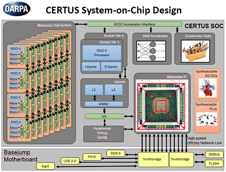
CERTUS System-on-Chip Design
To achieve that goal, the CERTUS team proposes to develop learning algorithms that spot and enhance ‘regularity’ in high-level descriptions, build sophisticated pipelines, and enable system architects to compose blocks, including analog blocks that are difficult to automate.
“We propose a synthesis methodology that targets not only the design tools but also the flow of design data across different tools that are akin to business processes,” said UCLA professor Mani Srivastava, noting that the project must take into account the role of commercial tools and third-party intellectual property (IP) in the design process. “Once micro-architectural design is complete, the flow through commercial tools proceeds rapidly but faces tortuous repetitions to close the ‘last MHz’ gap in performance.”
The project will focus on high-performance systems-on-chips that contain one or more processing elements, usually in the form of an IP block produced from commercial vendors and supported by publicly-available software development tools. In the first phase of the project, researchers will design and build an accelerator-centric SoC for use in autonomous vehicles under the Autonomy project with Northrop-Grumman Aerospace Systems and UC San Diego’s new Contextual Robotics initiative. In phase two, the focus will be on process porting issues, and the University of Michigan will take the lead on an ARM-hosted, accelerator-based implementation of the DARPA-selected SoC design (leveraging a decade-old research agreement between ARM and Michigan). The SoC will contain an array of processing cores based on the RISC V processor from Berkeley.
The CERTUS team is focused on devising compositional methods that allow systematic reuse of designed blocks, including high-performance analog circuit blocks.
At UC San Diego, Prof. Gupta pulled together a group from the Computer Science and Engineering (CSE) and Electrical and Computer Engineering (ECE) departments in the Jacobs School of Engineering. CSE-based faculty include Gupta himself and Michael Taylor (who was the lead architect of the DARPA-funded MIT Raw 16-core multicore processor chip). They will collaborate with ECE professors Patrick Mercier and Ian Galton (the inventor of a new type of high-performance, phase-locked loop, or PLL, implemented as the clock generator in the latest Qualcomm Snapdragon mobile processor) and Patrick. Other investigators on the DARPA project include UCLA’s Mani Srivastava, Cornell professors Zhiru Zhang and Christopher Batten, and Ron Dreslinski at the University of Michigan.
Gupta and Srivastava were, respectively, director and deputy director of the now-ending Variability Project funded by the National Science Foundation in 2010 under its Expeditions in Computing program.
Share This:
You May Also Like


Stay in the Know
Keep up with all the latest from UC San Diego. Subscribe to the newsletter today.