

Nanoshaping Method Points to Future Manufacturing Technology
Published Date
By:
- Emil Venere
Share This:
Article Content
A new method that creates large-area patterns of three-dimensional nanoshapes from metal sheets represents a potential manufacturing system to inexpensively mass produce innovations such as "plasmonic metamaterials" for advanced technologies.
The metamaterials have engineered surfaces that contain features, patterns or elements on the scale of nanometers that enable unprecedented control of light and could bring innovations such as high-speed electronics, advanced sensors and solar cells.
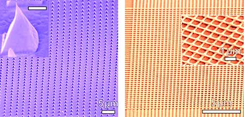
From left: scanning electron microscope images of silver nanopyramids and silver fish net fabricated by laser shock imprinting.
The new method, called laser shock imprinting, creates shapes out of the crystalline forms of metals, potentially giving them ideal mechanical and optical properties using a bench-top system capable of mass producing the shapes inexpensively.
Findings are detailed in a research paper appearing Friday (Dec. 12) in the journal Science. The paper is authored by researchers from Purdue University, Harvard University, Madrid Institute for Advanced Studies, and the University of California, San Diego. The research is led by Gary Cheng, an associate professor of industrial engineering at Purdue. Jian Luo, a professor of nanoengineering and materials science and engineering at the Jacobs School of Engineering at UC San Diego is one of the co-authors.
“This new technology, called “laser shock imprinting,” was originally invented and further developed by the Purdue team led by Prof. Cheng,” Luo said. “I was very excited when Gary told me this new technology back in November 2011 and asked me get involved to contribute a bit to the material science aspects of the investigation.”
“Both Gary and I are fascinated by the ability to deform crystalline metal foils very uniformly at nanoscale under ultra-high strain rates. We believe that this is a result of the interactions between grain boundaries and non-equilibrium defects generated by the laser shock, such as dislocations,” Luo said. “One hypothesis is that grain boundaries may undergo a disordering “phase” transition during the laser shock imprinting, which can facilitate the adsorption of non-equilibrium defects. Sponsored by a new National Security Science and Engineering Faculty Fellowship and earlier projects from various agencies, my research group has been investigating similar interfacial phenomena in a wide variety of metallic and ceramic materials with various different application backgrounds.”
The shapes researchers created include nanopyramids, gears, bars, grooves and a fishnet pattern, and are too small to be seen without specialized imaging instruments and are thousands of times thinner than the width of a human hair. The researchers used their technique to stamp nanoshapes out of titanium, aluminum, copper, gold and silver.
A key benefit of the shock-induced forming is sharply defined corners and vertical features, or high-fidelity structures.
"These nanoshapes also have extremely smooth surfaces, which is potentially very advantageous for commercial applications," Cheng said. "Traditionally it has been really difficult to deform a crystalline material into a nanomold much smaller than the grain size of starting materials, and due to the size effects the materials are super-strong when grain size has to be reduced to very small sizes. Therefore, it is very challenging to generate metal flow into nanomolds with high-fidelity 3-D shaping."
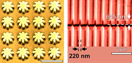
From left: scanning electron microscope images of an array of nanogears imporinted on cold-rolled aluminum foil and nanobars.
The researchers also created hybrid structures that combine metal with graphene, an ultrathin sheet of carbon promising for various technologies. Such a hybrid material could enhance the plasmonic effect and bring "metamaterial perfect absorbers," or MPAs, which have potential applications in optoelectronics and wireless communications.
"We can generate nanopatterns on metal-graphene hybrid materials, which opens new ways to pattern 2-D crystals," Cheng said.
The technique works by using a pulsed laser to generate "high strain rate" imprinting of metals into the nanomold.
"We start with a metal thin film, and we can deform it into 3-D nanoshapes patterned over large areas," Cheng said. "What is more interesting is that the resulting 3-D nanostructures are still crystalline after the imprinting process, which provides good electromagnetic and optical properties."
Whereas other researchers have created nanoshapes out of relatively soft or amorphous materials, the new research shows how to create nanoshapes out of hard and crystalline metals.
The silicon nanomolds were fabricated at the Birck Nanotechnology Center in Purdue's Discovery Park by a research group led by Minghao Qi, an associate professor of electrical and computer engineering.
"It is counter-intuitive to use silicon for molds because it is a pretty brittle material compared to metals," Qi said. "However, after we deposit an ultrathin layer of aluminum oxide on the nanomolds, it performs extremely well for this purpose. The nanomolds could be reused many times without obvious damage. Part of the reason is that although the strain rate is very high, the shock pressure applied is only about 1-2 gigapascals."
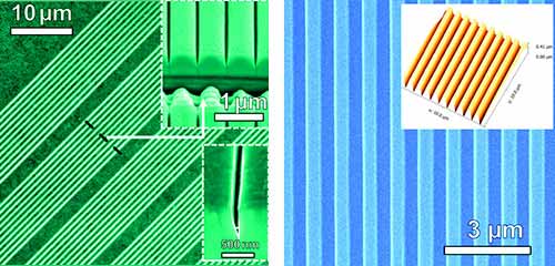
From left: scanning electron microscope images of an array of triangular V-grooves and an array of nanotrenches in a titanium thin film.
The shapes were shown to have an "aspect ratio" as high as 5, meaning the height is five times greater than the width, an important feature for the performance of plasmonic metamaterials.
"It is a very challenging task from a fabrication point of view to create ultra-smooth, high-fidelity nanostructures," Qi says. "Normally when metals recrystallize they form grains and that makes them more or less rough. Previous trials to form metal nanostructures have had to resort to very high pressure imprinting of crystalline metals or imprinting amorphous metal, which either yields high roughness in crystalline metals or smooth surfaces in amorphous metals but very high electrical resistance. For potential applications in nanoelectronics, optoelectronics and plasmonics you want properties such as high precision, low electromagnetic loss, high electrical and thermal conductivity. You also want it to be very high fidelity in terms of the pattern, sharp corners, vertical sidewalls, and those are very difficult to obtain. Before Gary's breakthrough, I thought it unlikely to achieve all of the good qualities together."
The paper was authored by Purdue doctoral students Huang Gao, Yaowu Hu, Ji Li, and Yingling Yang; researcher Ramses V. Martinez from Harvard and Madrid Institute for Advanced Studies; Purdue research assistant professor Yi Xuan, Purdue research associate Chunyu Li; Jian Luo, a professor at the University of California, San Diego; Qi and Cheng.
Future research may focus on using the technique to create a roll-to-roll manufacturing system, which is used in many industries including paper and sheet-metal production and may be important for new applications such as flexible electronics and solar cells.
“It is important to emphasize that the exact underlying mechanisms that enable this laser shock imprinting process, including whether grain boundary disordering indeed occurs and plays a role, remain elusive, which are subjects of future research that Gary and I are interested in pursuing via a continuing collaboration,” Luo said.
The work was supported by the National Science Foundation, National Institutes of Health, Defense Threat Reduction Agency, Office of Naval Research and the National Research Council.
Share This:
You May Also Like


Stay in the Know
Keep up with all the latest from UC San Diego. Subscribe to the newsletter today.